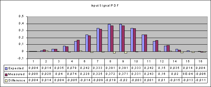
Figure 01: PDF test expected output
By Olivier Gentaz
June, 2000
II TEST BENCH OVERVIEW
II.1 Tests to be performed
II.1.1 Probability Density Function
Assuming a gaussian input signal at the nominal input level, the 16 comparators thresholds of the digitizer should be equally distributed over the dynamic input range such as a data amplitude histogram will produce a gaussian probability density function (PDF).
Measurement of the samples statistical distribution will show whether
each individual comparators works properly or not at high speed.

Figure 01: PDF test expected output
II.1.2 Stability Vs Time
The autocorrelation sequence zeroth lag is an image of the signal power. Its time stability is of prime importance in our application as data integration time may vary up to several minutes. It can be estimated according to the Allan variance of the sampled data.
This test will point out a possible abnormal drift of the input analog stage and one be able to estimate the corresponding correlator maximum integration time which can be expected by using this chip.
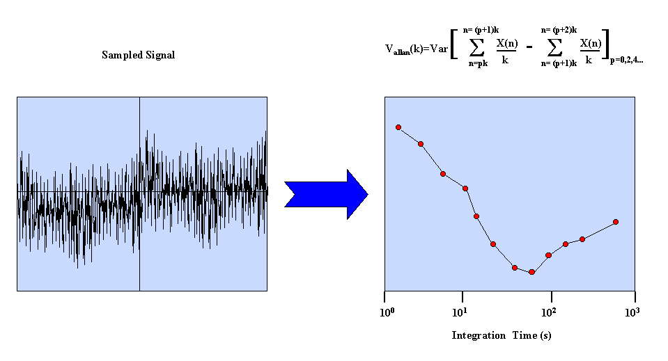
Figure 02: Drift Measurement
II.1.3 Sampler frequency response
The input signal being a white noise, the autocorrelation FFT should
be a flat response. In practice, one would obtain a low-pass response including
ripple within the passband (due to the input buffer mismatch for instance).
In fact, the computed FFT corresponds to the frequency response of the
whole digitizer stages and would underline an excessive frequency distortion
of this stages.
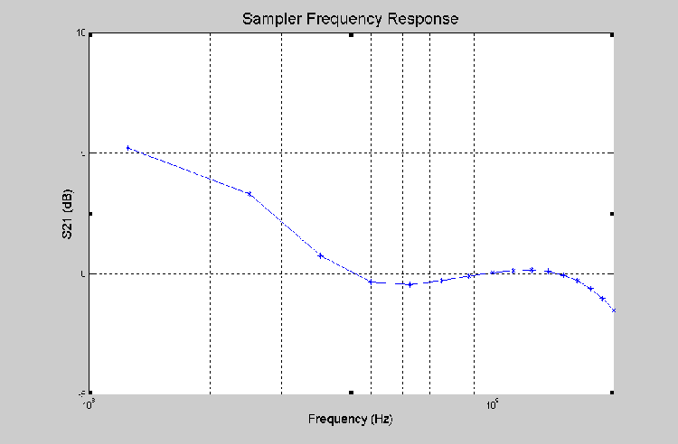
Figure 03: Sampler frequency response example (4GHz sampling clock-16 Lags)
II.1.4 Measurements precision
One would reach a 0.1% precision on the estimated autocorrelation Cxx,. Hence, the minimum number of acquisitions N must be:
![]()
II.2 Physical architecture
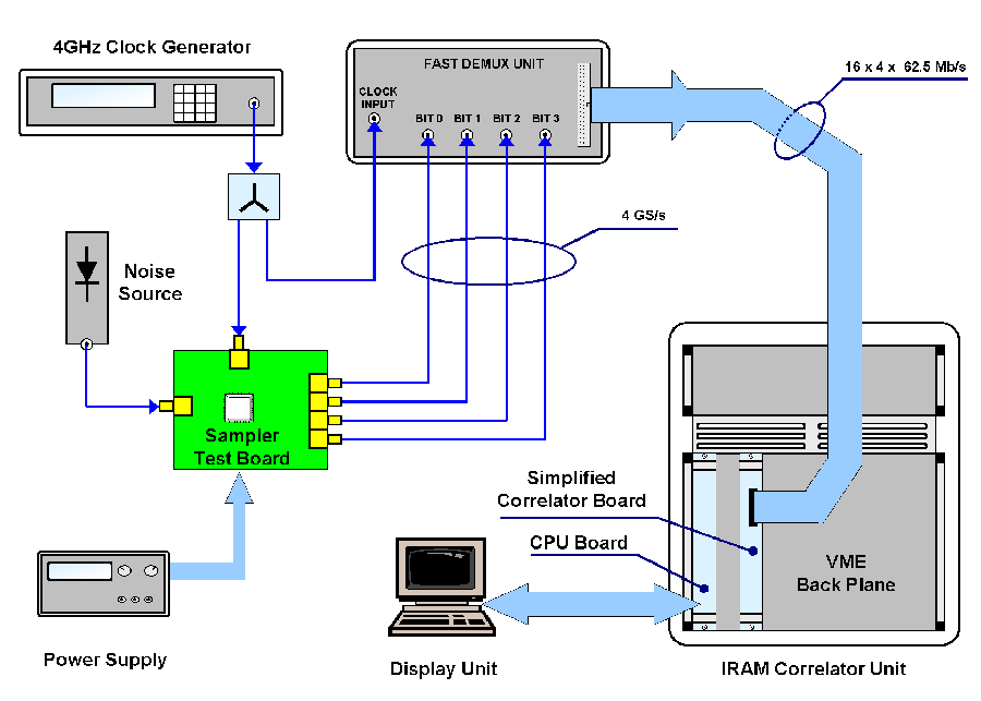
Figure 04: Test Bench Physical Architecture
The test bench is made up of both commercial instruments (clock generator, power splitter, noise source, power supply, VME sized CPU board, display unit) and home made units (fast demultiplexing unit, simplified correlator board, IRAM correlator unit).
The clock generator will deliver a working frequency up to 1.3 time the nominal sampling frequency (4GHz). The noise source shall be flat over the input frequency range and will be able to deliver an output level of 0dBm over a 2GHz bandwith (-33dBm/MHz). The sampler chip will be powered thanks to an adjustable power supply to measure the input stage gain stability vs power supply. Cable lengths will be carefully choosen in order to overcome the signal timing between sampler test board and the demux unit.
The autocorrelation number of lags is set to 16 which represents a good compromise between complexity and performance. Thus, the fast demultiplexing unit (FDU) acquires a set of 16 consecutive samples at a rate of 4GS/s. Once samples have been captured, they are distributed at a lower rate into several parallel data flow able to be off-line processed by the simplified correlator board.
The simplified correlator board (SCB) is in charge of the 16 lags autocorrelation computation and also of the PDF measurement. At the present time, these two functionalities will not be avalaible simultaneously on the board for practical design reason. Regarding the wanted test, the corresponding FPGA configuration EPROM should be set on board.
Once computation has run over the number of settled acquisitions (according
to the wanted accuracy), the final result is sent out of the SCB trough
the VME bus to an OEM CPU board. This latter supports the test software
which computes the Van Vleck correction then the FFT and displays results.
In order to be able to instantaneously observe the effect of whatever change
(on-board adjustement, temperature step, etc
), an FFT display refreshing
rate of once per second will be implemented.
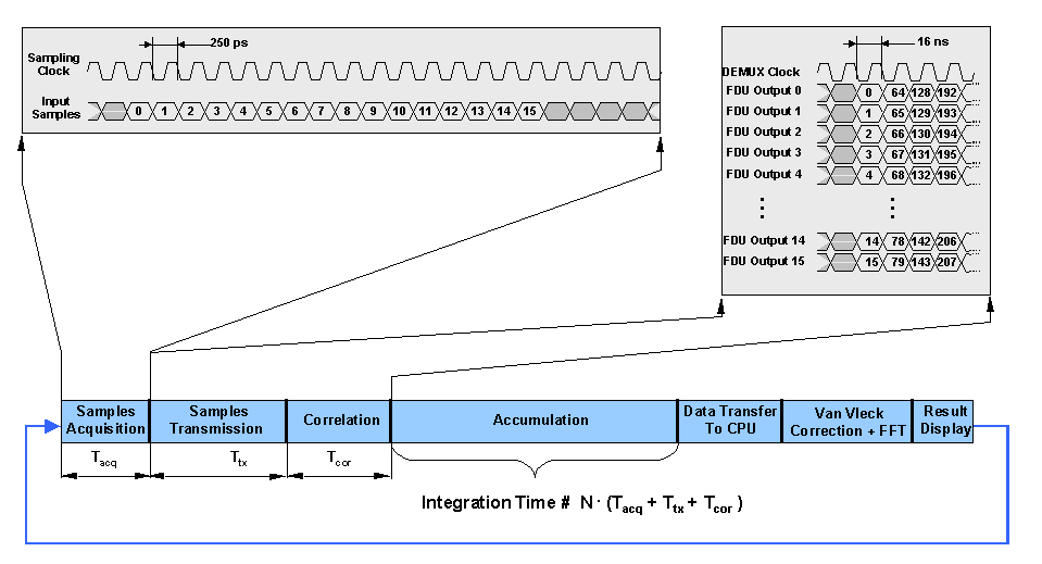
Figure 05: System Time Sequence
II.2.2 Connectors requirements
Regarding the ultra high frequency input and output rates, 50W SMA connectors are mandatory on the sampler test board. Its Power supply connector remains TBD.
The fast demultiplexing unit uses one SMA connector per input bit whereas
its output data flows are sent to the SCB input via high density multipoint
connectors together with twisted-pair cable
III HARDWARE IMPLEMENTATION
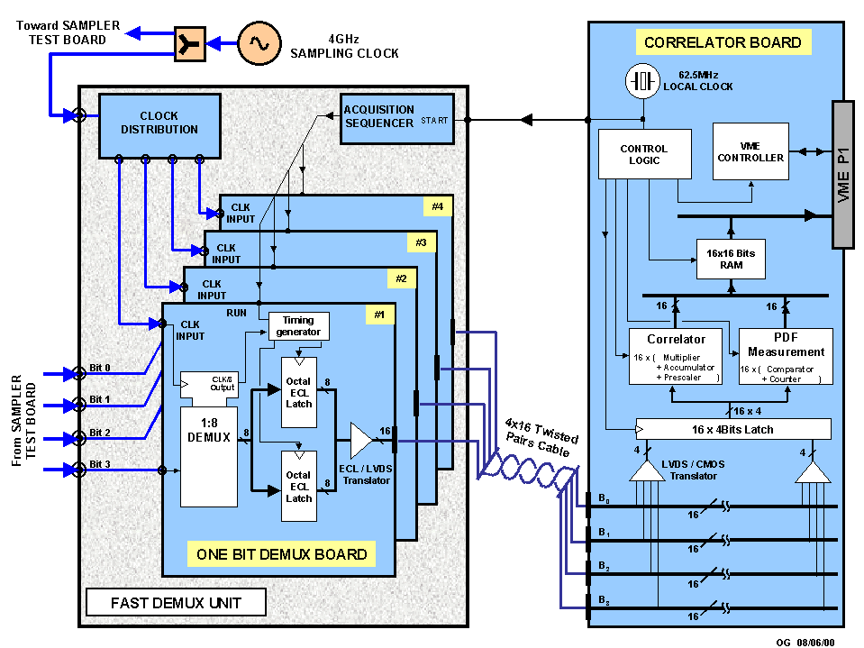
Figure 06: System Block Diagram
Samples acquisition and processing are respectively performed by the
FDU and the SCB. Following an acquisition request from the SCB, the 16
samples packet is parallely transmitted toward the SCB . This asynchronous
transmission gives advantage of being able to run the FDU with a varying
sampling clock independent of the SCB processing speed.
III.2 FDU
Regarding the fact the sampler resolution could change and that ultra high frequency are involved in this unit, a one board per bit architecture is choosen.
A single demultiplexer board is composed of a 5Gb/s GaAs 1:8 demux (NEL Product) as a first layer. Its 500Mb/s output rate is downconverted to 62.5Mb/s thanks to a second layer made up of two sets of 8 bits register alternatively latched. This final rate results from a preliminary analysis on the maximum input rate of the FPGA which implements the correlation.
Once the 16 data packet has been captured, it is transmitted to the
SCB thanks to differential line drivers.
III.3 SCB
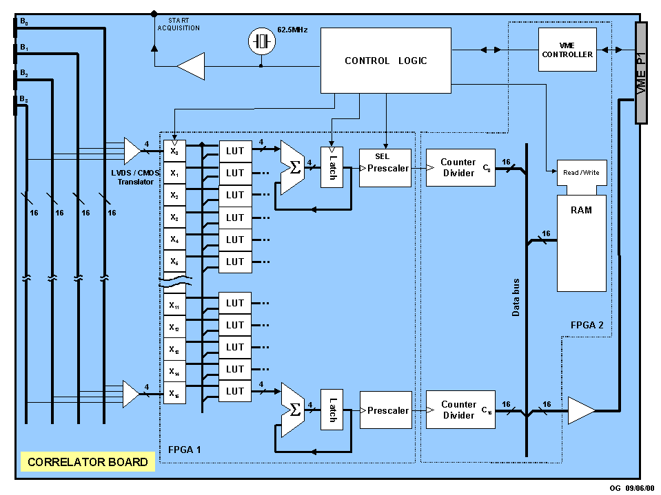
Figure 07: SCB general block diagram
Autocorrelation and PDF measurement are physically computed thanks to the same digital circuits. The only difference between these two operations lies in the look-up table (LUT) contents. When using the circuit to compute the autocorrelation, LUTs are downloaded with the optimal multiplication table whereas using the circuit to measure the PDF, LUTs are downloaded such as they can be seen as a set of 16 comparators, each dedicated to the occurrence count of a particular level.
As a first analysis, the whole operations will be implemented thanks to two FPGA (ALTERA Products) together with miscellaneous standard digital circuits according to the figure above. This leads to an SCB size of one VME board.