
The Wideband Line Multiple Autocorrelator (WILMA)
The focal plane array receivers of the Pico Veleta deliver 18
IF bands, every one being one GHz wide. The pre-existent
autocorrelator,
VESPA, is very flexible, but does not offer the possibility of
processing
the totality of the bandwidth delivered by the receivers. For this
purpose
a special spectrometer has been designed, which has no flexibility at
all,
but which is capable of crunching all the bandwidth at once.
Architecture
The signal is delivered in the 100 to 1100 MHz range, to be
compatible
with the already existing spectrometers. This is not fortunate because
an up-conversion is necessary, in order to reduce the relative
frequency
range. An Image Rejection Mixer (IRM) changes the 1 GHz band into
two 500 MHz subbands. Both USB and LSB are converted to digital (full
2-bit)
after lowpass filtering and level adjustment. The digitized data (1024
Ms/s) is conditioned to a lower frequency, re-ordered and transmitted
to
the correlator boards pairs, which are clocked at 128 MHz.
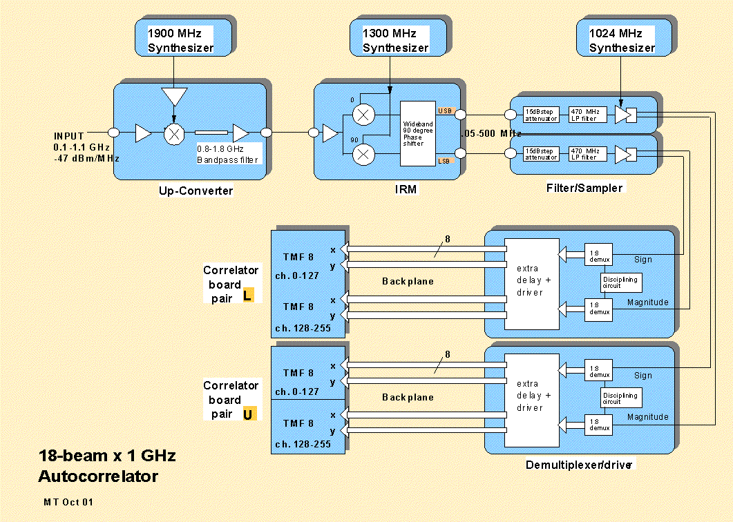
The whole system has been squeezed in a single rack :
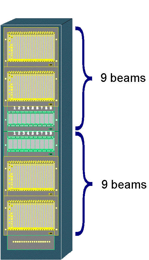
Its total power consumption is 2.4 KW
Technical description, by module :
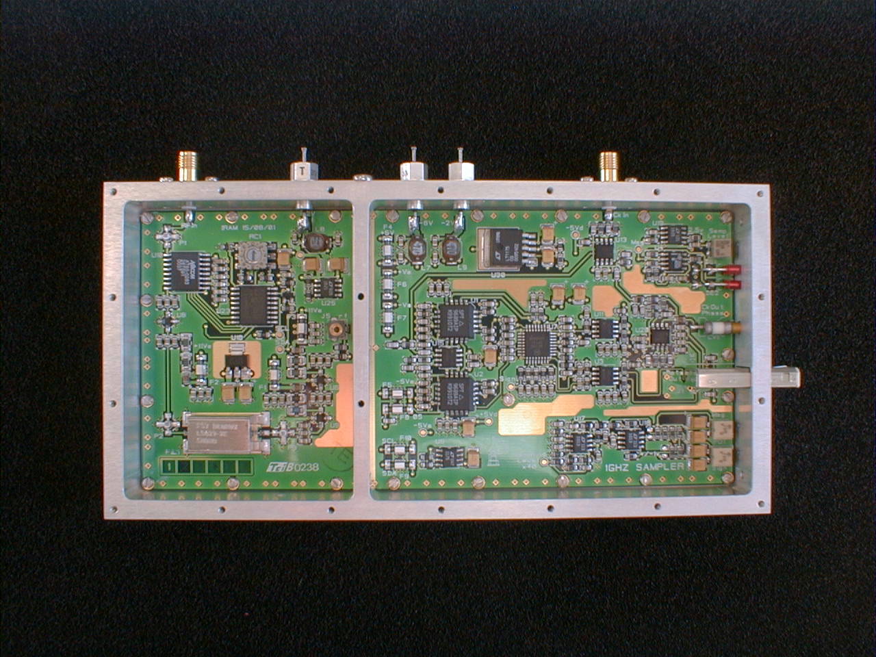
1Gb/s 1:8 Demultiplexer (view image)
The purpose of this board is to receive a dataflow at 1 Gigabit/s and to deliver 8 dataflows at 128Mbit/s to slower standard commercial electronics.
This board receives a digital dataflow at 1 Gigabit/s from the
sampler,
a 2-bit data and a 1024 MHz clock. After translation from NECL to PECL
levels, the 2 bits are demultiplexed by two independent MAX3680. They
deliver
in LVTTL levels two 8-bit dataflows and their associated 128 MHz
clocks,
which are randomly phased at power-up. These 128 MHz clocks go in a
synchronisation
detector. Until clocks are synchronized, the detector requires from the
1024 MHz clock divider of the modulus demultiplexer, to drop one cycle.
The modulus data timing is automatically disciplined to the sign timing
in less than 8 tries at power up. A red LED on each module indicates if
this mechanism has failed.
Then data flows into an FPGA (EPF10K10A) which generate
immediate and delayed dataflows that are buffered and sent to the
correlator
boards through the P2 backplane. A 128 MHz clock is also delivered to
the
two correlator boards that are involved with each demux board. Pairs of
correlator boards may receive 128Mhz clocks of different phases, at
random.
Boards have a 3U-VME format and are located at the rear of the
rack.
This board also carries the I2C bus from the P2 backplane to the
sampler.
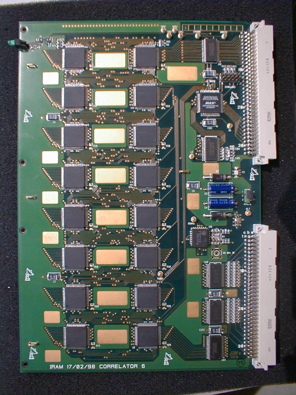
Correlator boards (view image)
The correlator boards are the same ones that have been used for the Plateau de Bure interferometer correlator. They are operated with a time-multiplex factor of 8. Actually they work in cross-correlation, but they ignore that the demux/driver board delivers to them the same signal (with a half-length delay) on both inputs. They are populated with IRAM correlator chips, and are described in more detail here.
This configuration is summarized in the zero flexibility table
below :
| Bandwidth | Sub-band | Time Multiplex Factor | Lags number | Real channels | Channel spacing |
| 18 x 1024 MHz | LSB + USB | 8 | 18 x 512 | 18 x 512 |
|
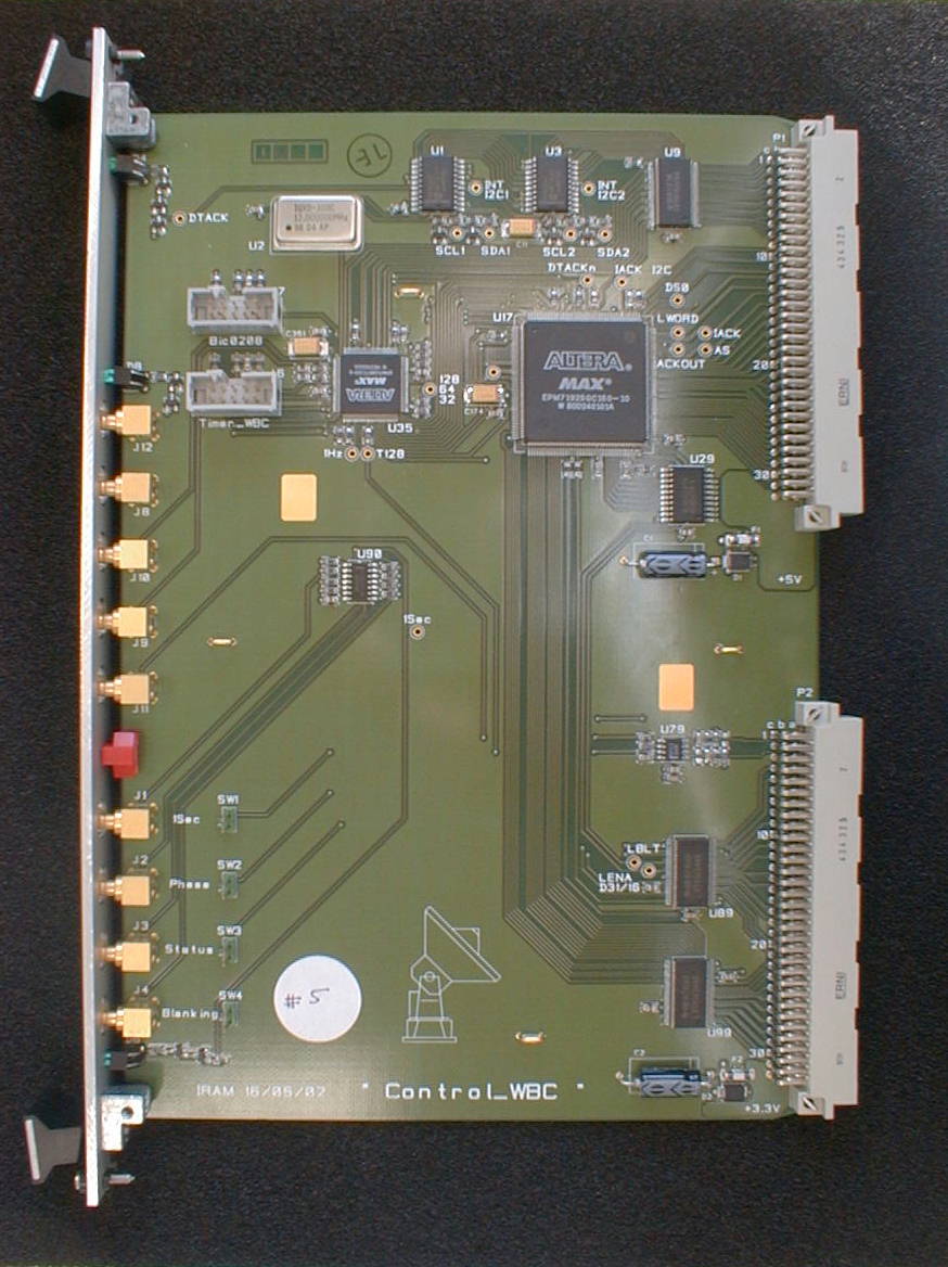
Control board (view image)
1) The timing interface
The input signals are :2) The VME bus interface
BLANKING STATUS PHASE 1SEC
An EPM7128 FPGA receives the inputs and delivers correlator timing signals under the supervision of a control register. Three acquisition rates can be selected : 128 Hz, 64 Hz or 32 Hz.
It also feeds the VME controller with interrupt requests.The output signals are :
LDRST for the correlator INHADD for the correlator A 128 MHz clock for test A 128/64/32 Hz clock for test A 1 Hz signal for test if used
The VME controller is an EPM7192 FPGA that decodes the address of this board plus all the boards of the unit, generates 4 interrupts and send the DTACK to the CPU.2) The I2C bus interfaceThe 4 interrupts are :
1 : STATUS 2 : PHASE 3 : 128/64/32Hz 4 : I2C interface
Two PCF8584 I2C bus controllers are used to handle 9 sampler
addresses.
Boards have a 6U-VME format and are located at the front of the rack.
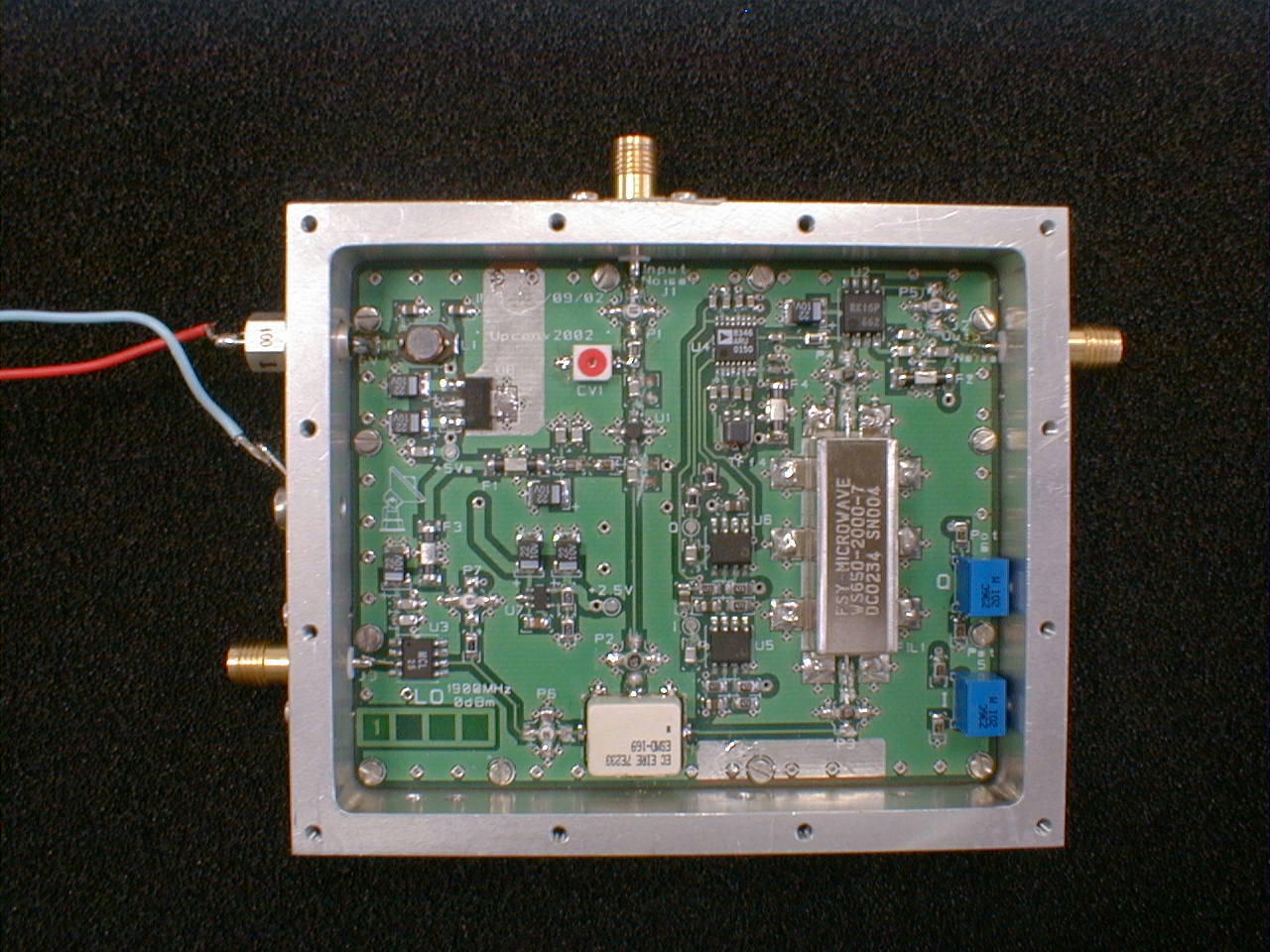
Up-converter (view image)
The input frequency range (0,1 to 1.1 GHz) needs to be
converted
to a range acceptable by the SSB mixer. A fixed LO at 1900 MHz is used.
The output is from 800 to 1800 MHz. Since the input and output ranges
do
overlap, (from 800 to 1100 MHz) the design has been optimized to the
best
RF-to-IF isolation of the mixer. The resulting LO leakage at 1900 MHz
is
quite important and would lead the following stages to misfunction, so
a special circuit has been implemented for its cancellation. It makes
use
of an I/Q modulator, controlled by two potentiometers, that are
individually
adjusted to reduce the leakage to less than one channel power level.
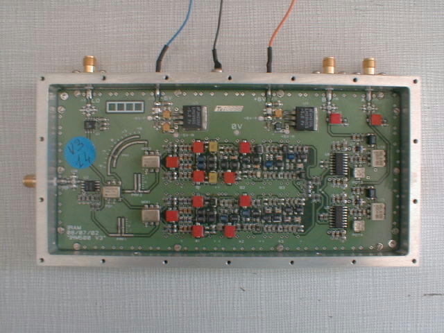
IRM modules (view image)
Image Rejection Mixers (also called SSB mixers) are used to convert the 0.8-1.8 GHz IF band into a pair of basebands, from 100 kHz to 470 MHz. They receive a 1300 MHz LO from a local synthesizer. They make use of a wideband 90 degree phase shift LC network. The 100 kHz cutoff frequency causes a discontinuity in the spectrum at the center of the band. To observe a spectral feature of interest, it is wise to place it not exactly at the center of the band, but a few tens of MHz apart.
Samplers (view image)
The samplers operate in full 2-bit mode at 1024 MHz rate. Its analog
section features an amplifier and a 470 MHz (@-3dB) low-pass filter for
antialiasing. A programmable (via I2C) attenuator allows to
adjust
the input level to the optimal RMS value, by 0.5 dB steps over a 15.5
dB
range. On the back panel, two LEDs indicate either too low or two
high input voltage. This is useful for quick visual debugging.
The digitized signals are transmitted down to the demux boards. On
the same connector, the sampling clock and the I2C controls are sent up
to the sampler.
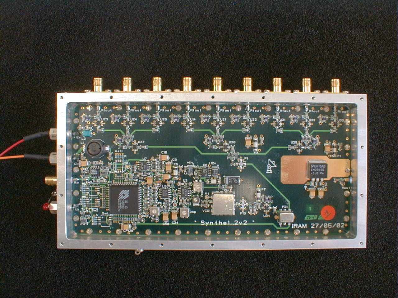
9-output synthesizer (view image)
Wilma requires oscillators at 1900,1300,and 1024 MHz, each of
them delivering 9 copies. A single design has been made for all
purposes,
only differing by the settings of the synth chip, and the VCO for the
1900
MHz unit. They are locked on the 10 MHz from the station. There
are
two synthesizers in the Upconverter crate, and three in each
IRM/Sampler
crate. On each crate there is a 10 MHz outer BNC connector with
an
impedance of 150 Ohms. The three crates should be connected in parallel
to one output of the standard. Inside a crate, a buffered daisy-chain
with
SMA cables is implemented.
This machine has been built and installed on the Pico Veleta
observatory
by November,2003. Another correlator slice of 1 GHz has been
simultaneously
built for the observatory of Yebes. It has been named Peebles.