A 4GS/s
Sampling Head
for the next
generation PdBI wideband correlator
Olivier GENTAZ IRAM/Back-End
September 2006
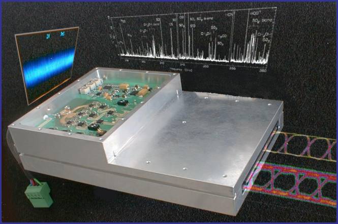
The new generation of receivers that will be soon installed at the PdBI delivers a 4GHz IF
bandwidth (from 4 to 8 GHz). The future wideband
correlator being expected to have an input frequency range of 2 to 4 GHz, a
Sampling-Head that performs 2-Bit/4-Level band-pass sampling at 4GS/s has been
developed. This assembly has been named “SHERIF” (Sampling Head Extending
Range of Iram Facility). It makes an extensive use of
very-high-speed COTS(*) chips from well-known semiconductors
manufacturers. These whole chips are SiGe-based and are today ready-made and available for
sale. You will find hereafter a detailed description of the assembly.
(*): “Commercial Off-The-Shelf”
1. Target Specifications
The table
below lists the specifications that have been settled prior to start the
design.
|
|
Parameter |
Condition |
Value |
Note |
|||||||||||||||||
|
Functional Specifications |
Quantization Scheme |
|
2-Bit / 4-Level |
The 3 sampling thresholds are adjustable |
|||||||||||||||||
|
Digital Outputs Time Demultiplex Factor |
|
16 |
Compelled by COTS Demux chip |
||||||||||||||||||
|
Output Coding |
|
Sign/Magnitude -V1
V0 +V1
|
|
||||||||||||||||||
|
Output Logic Levels |
All Outputs terminated with 100W differential load |
LVDS standard |
Compelled by COTS Demux chip |
||||||||||||||||||
|
Performance Specifications |
Sampling Rate |
|
4GS/s Min |
|
|||||||||||||||||
|
Analog Input Bandwidth |
|
2GHz to 4GHz Min |
|
||||||||||||||||||
|
Analog Input Bandwidth Ripple |
|
1dBPeak-Peak Max |
This value limits the SNR loss to 0.4% |
||||||||||||||||||
|
Analog Input Bandwidth Slope |
|
1dBEdge-Edge Max |
This value limits the SNR loss to 0.2% |
||||||||||||||||||
|
Analog Input Level |
|
-20 dBm to 0 dBm |
0.5dB step adjustment |
||||||||||||||||||
|
Analog Input Return Loss |
2GHz £ Fin
£ 4GHz |
14 dB Min |
(14dB Û SWR £ 1.5) |
||||||||||||||||||
|
Sampling Clock Input Level |
|
0dBm±3dB |
|
||||||||||||||||||
|
Demultiplexing Clock Input Level |
|
0dBm±3dB |
|
Table 1.1: Target Specifications
Beyond electrical performances, special attention has
been paid to the mechanical design in order to get a compact assembly able to
be slipped into its “Delay-Data Format Conversion” motherboard.
2. Block Diagram
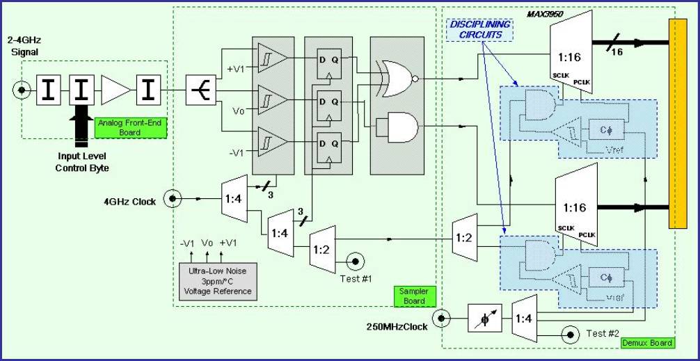
Fig 2.1: Sampling-Head
Schematic Block Diagram
The sampling head assembly has been divided up
into 3 physical units, each corresponding to the main functions of a
Sampling-Head: conditioning and digitizing the signal, then lowering the output
data rate.
This modular approach
1) Provides a high
RF isolation between blocks (at the expense of a careful mechanical design).
2) Allows for individual design and test of the different blocks helping thus to minimize the unfeasibility risk.
The classical Flash
architecture has been adopted for the sampler
block. The Demux board makes use of two independent
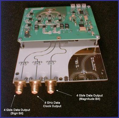
3. Physical Implementation
The picture
hereafter shows the sampling-head prototype assembly
under different views.
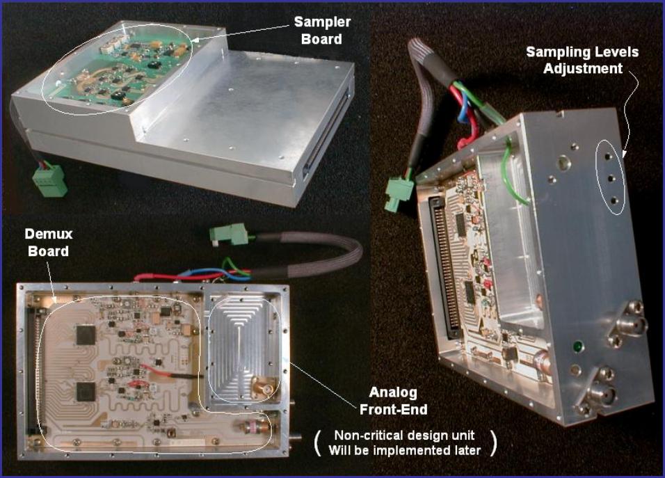
Fig 3.1: Sampling-Head Assembly
Overview
Signals are
transmitted from the housing upper deck to the lower deck via a buried coaxial
link or a stacked high-speed differential connector.
Though the
majority of the parts are digital devices, microwave design rules have been applied
in order to make sure the selected very high-speed chips can fully express
their performances. The assembly housing has been designed as compact as
possible in order to shorten the distance between high-speed devices. Moreover,
controlled line lengthening both on sampler and demux board ensures the set-up
and hold time requirements of the chips are met without the need of an
adjustment that would likely be very touchy @ 4Gb/s.
3.1 The Sampler Board
The Sampler board
converts the 2-4GHz band into a 2-Bit/4-Level data stream @ 4GS/s thanks to 3
ultrafast comparators followed by a set of high-speed digital chips. Chips are
interconnected with differential microstrips and interfaced with high-speed
differential logic standards (CML, PECL, etc…)
The conversion is performed according to 3
adjustable sampling thresholds. Once these thresholds are properly adjusted,
the sampling-head delivers a stable near-perfect sample
statistical distribution leading the correlator to operate with its maximum
efficiency.
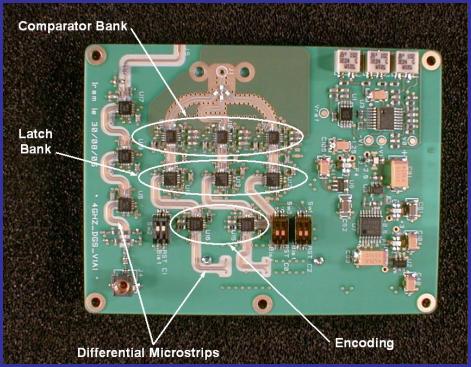
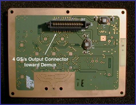
Fig 3.2: The Sampler Board Top Face Fig 3.3:
The Sampler Board Bottom Face
3.2 The Demux Board
|
The
Demultiplexer board converts the 4GS/s incoming serial data stream into 16
parallel LVDS data streams @ a 250MHz rate. A data being
made up of 2 bits, 2 independent demux chips are implemented. As the selected
chips have their own internal clock divider, each divider can be set in any
state amongst the 16 possible states at power-up. This may lead to have an
output data misalignment from one demux to the other. This uncertainty about
the proper alignment of the output data is not only unacceptable for
repeatability concerns (the timing adjustment for a proper output data
capture would be drastically tightened) but also because it may generate
scalloping in the output data spectrum up to a crippling level. So, a
disciplining circuit has been implemented. Just as a PLL ensures the phase of
a VCO is locked to the phase of an external clock reference, this circuit
ensures that the whole set of the output data are always aligned in time with
respect to the incoming correlator clock. This may be seen as a “discrete”
PLL being able to work only with a finite number of phase states. |
|
Fig 3.3: The Demux Board Top Face
|
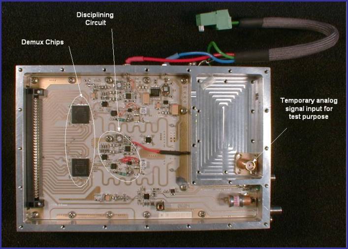
3.3 The Analog Front End Board
The AFE board controls the input power
thanks to a 0.5dB step digital attenuator that fits the input signal amplitude
to the sampling thresholds. It will also eventually compensate for the band
slope of the incoming IF signal.
This board will be made up of common
broadband RF devices and several sources have been identified for these
devices. Therefore, provided that usual microwave design rules are applied, its
implementation is not risky and will be done later once the spectral properties
of the incoming IF signal will be known with accuracy.
4. High-Level Test
Equipment
Physical layer tests usually
performed with RF generators and oscilloscopes can only ensure that the data
electrical characteristics are compliant to the needed transmission standard
(ECL, CML, LVDS, etc…). In order to determine the meaning of the generated bit
flow, high-level tests must be performed once the different boards have been
integrated within the assembly housing.
For this purpose,
the IRAM Digitizer Test Equipment (DTE)
developed for the
The test equipment has
been integrated within a rack providing thus a Stand-Alone unit suitable for both test & production phases
2) Finer resolution of the
test correlator
Thanks to a higher
capacity FPGA, the previous 192 channels resolution has been raised up to 320
channels, i.e. 6.25MHz channel spacing
@ 2GHz bandwidth
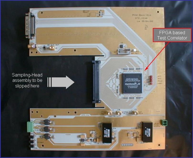
Fig 4.1: The Test Autocorrelator Board
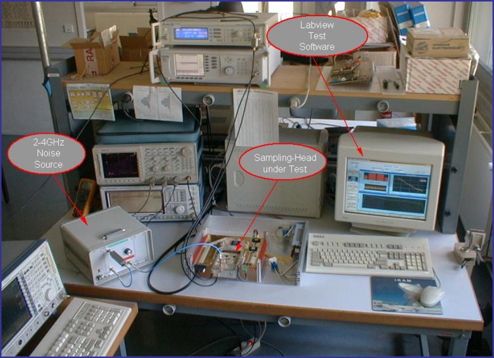
Fig 4.2: The Sampling-Head
Test Setup
This equipment performs the following measurements:
- Statistical distribution
of the input samples
- Frequency response
(ripple and flatness)
- Stability over time
(Allan variance)
These high- level characteristics give a complete qualification of the
Sampling-Head module
5. Test Results
5.1 Preliminary Measurements
5.1.1 Sampler Board
|
Fig 5.1: Sampler Test
Board
|
Fig 5.2: Sampler
Output Eye Diagram @ 4GHz (Sign Bit) |
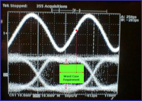
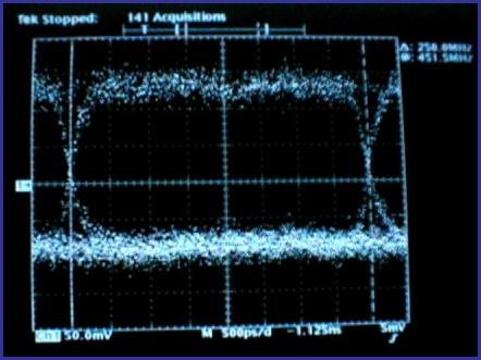
The rise/fall
times of the sampler output eye diagram are oscilloscope limited (chip
specification: 60ps max). Nevertheless the eye opening at the demux input stage
meets the worst-case requirements with
margin (amplitude must be outside the green area, clock can
toggle anywhere within the figure 5.2 green area).
5.1.2 Demux Board
The proper
functioning of the disciplining circuit can be seen on the two figures below.
The figure 5.3
shows the phase comparator output of the disciplining circuit in motion. This
measurement is done with a sliding 250MHz clock such as the disciplining
circuit is constantly seeking for a stable phase state. Thanks to the display
persistence, one can see that all the possible phase states are swept.
The
figure 5.4 shows the phase comparator output of the disciplining circuit during
a random phase-seeking sequence triggered by power-up. The mean time to
phase lock is » 6ms.
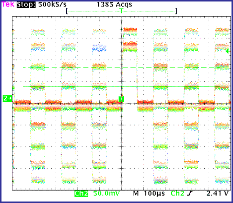
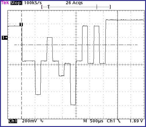
Fig 5.3: A Demux Phase States Grid Fig
5.4: A Demux Typical Phase Seeking Sequence
The two figures
hereafter shows the demux output eye diagram.
The figure 5.5
has been performed with a fast oscilloscope to avoid rise/fall time measurement
to be limited by instrumentation. The eye diagram is ringing-free,
outstandingly opened and LVDS compliant.
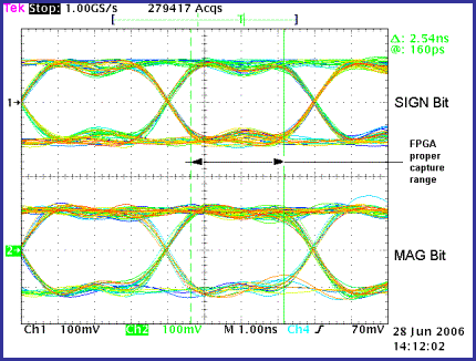
The figure 5.6 aims
to check whether the Sign-Bit and the Mag-Bit data are properly aligned. More
over, the FPGA input data capture range measured
thanks to the DTE has also been transposed on this figure showing a 60%
safe load for data capture.
|
Fig 5.5: The Demux Output Eye Diagram @ 250MHz
|
Fig 5.6: Alignment of the Demux Output Data
|
5.2 High-Level
Characterization
5.2.1 Validity of the captured Data
Prior to any data
analysis, the coherence of the 16 demux channels is checked: the statistical
mean and standard deviation of each demux output are computed and compared to
their expected theoretical values, getting therefore the “Offset relative error” and
“Amplitude relative error”.
If the demux
are properly working as a whole, the data delivered over the 16 channels must
have the same statistical properties. This can be seen hereafter on the screenshot of the
“Probability Distribution Function Viewer”. This software displays the offset relative error and amplitude relative error of each channel like a vector. The whole set of the
16 vectors is displayed on an XY chart (“error constellation”) and if all the demux
outputs are properly aligned, all vectors must be collinear. Any vector whose
magnitude or direction is significantly different from the others will point
out a data misalignment of the corresponding channel (likely due to a timing
corruption). Such a display provides a very useful global indicator to
instantaneously assess the complete working of the assembly under test.
The input data capture range of the FPGA that process the samples have
been measured to be 2.5ns over the 4ns clock period.
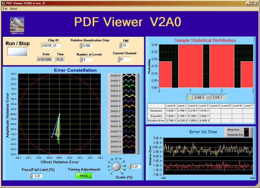
Fig 5.7: Data Alignment Check of the 16 Demux
Channels @ 250MHz
On the screenshot
hereunder, all the vectors are well within the 0.2% error limit (red circle)
and grouped toward the same direction. This measurement definitely validates the sample output coding and the
demux synchronization circuits.
5.2.2 Global measurement
The test software is performing 3 measurements that are displayed
together on the figure 5.8 hereafter:
2) The frequency spectrum of the sampler input signal
through FFT of the sample autocorrelation.
3) The Allan variance to measure the sampler gain
stability over long term.
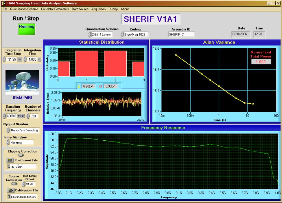
Fig 5.8: The Test Software GUI Global View
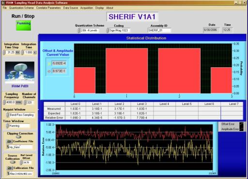
5.2.3 Threshold Spacing and Allan Variance
|
Fig 5.9: Sample Statistical Distribution Measurementafter thresholds adjustment |
|
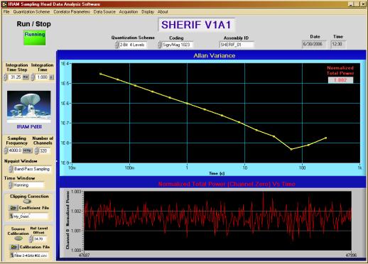
Fig 5.10: Allan Variance Measurement
|
|
The three sampling levels can be accurately adjusted to the optimal levels.
As they are independent, they can compensate for any of the three comparators
offset that would otherwise generate an asymmetry of the sample statistical
distribution. The measurement here below shows that after adjustments, errors
on each individual distribution bins can be lowered down to 10-3. The measurement is performed with a –1.5dBm power at the sampler
input. This power level corresponds to sampling levels that should be ±56.8mV
(@ V/s=0.906). At the comparators input, the measured
sampling levels are: At first sight, this input level range should be compatible with the IF Processor outputs after addition of a front-end amplifier module. |
|
The Allan variance displayed on the figure 5.10 measurement
shows a gain stability up to 64s. For integration times up to 128s, the DG/G standard deviation remains even lower than 10-4.
Thus, like it is, this module is suitable for single dish observations. This measurement is performed in a lab environment. Under a controlled
temperature environment, this stability is expected to be better yet. |
5.2.4 Frequency Response
|
Fig 5.11: Input Noise Source Spectrum measured
with an
R&S FSEB spectrum analyzer
|
|
Fig 5.12: Input Noise Source
Spectrum
without calibration
|
|||
|
The sampling-head is fed with gaussian noise from a 2-4GHz noise
source whose spectrum has been previously
measured with a spectrum analyzer (figure 5.11 measurement). |
|
On the figure 5.12 screenshot, the filter skirts can be identified (FcL=2.1GHz, FcH=3.9GHz) and within the bandpass, the displayed spectrum shape clearly meets the figure 5.11 measurement. |
||
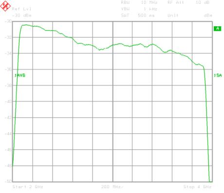

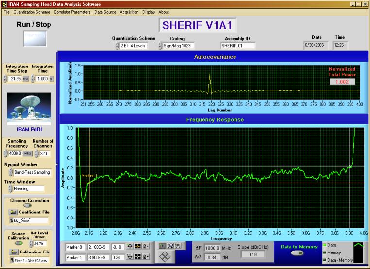
Fig 5.13: The Sampler
Calibrated Frequency Response
The sampler calibrated frequency response is deduced from the subtraction
of the measured noise source spectrum to the spectrum computed from the
autocorrelation.
Within the bandpass, the slope is ~ +0.4dB and the ripple is ~ ±0.2dB.
5.3 Overclocked Operation
Overclocking digital boards is a simple and pretty good way to estimate
the margins of a design.
The sampling head has been overclocked up to 8GHz (see
screenshot here below) with reduced performances (offset non-cancellation,
increase of the noise floor). This outstanding result just demonstrates that
the digital parts implemented on boards offer great margins that will ensure a
good production yield of the assembly as well a high level of quality for the
sampler data @ 4GS/s.
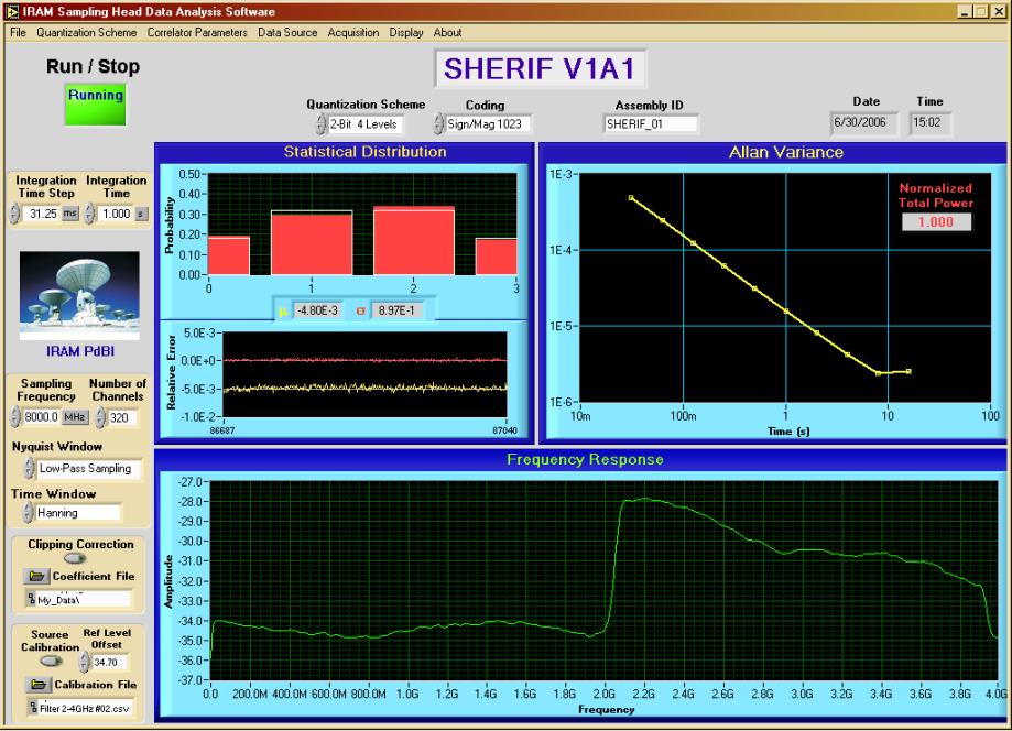
Fig 5.14: Low-Pass Sampling Operation @ 8GHz Sampling Frequency
5.4 Measured Characteristics
|
|
Parameter |
Condition |
Target
Value |
Measured Value |
Compliance |
|||||||||||||||||||||||||||||||||||
|
Functional Specifications |
Quantization Scheme |
|
2-Bit / 4-Level |
2-Bit / 4-Level |
Pass |
|||||||||||||||||||||||||||||||||||
|
Digital Outputs Time Demultiplex Factor |
|
16 |
16 |
Pass |
||||||||||||||||||||||||||||||||||||
|
Output Coding |
|
Sign/Magnitude -V1 V0
+V1
|
Sign/Magnitude -V1 V0
+V1
|
Pass |
||||||||||||||||||||||||||||||||||||
|
Output Logic Levels |
All Outputs terminated with 100W differential load |
LVDS standard |
LVDS standard |
Pass |
||||||||||||||||||||||||||||||||||||
|
Performance Specifications |
Sampling Rate |
|
4GS/s Min |
100MS/s to 8GS/s |
Over Pass |
|||||||||||||||||||||||||||||||||||
|
Analog Input Bandwidth |
|
2GHz to 4GHz Min |
DC to 6GHz |
Over Pass |
||||||||||||||||||||||||||||||||||||
|
Analog Input Bandwidth Ripple |
|
1dBPeak-Peak Max |
0.4dBPeak-Peak |
Pass |
||||||||||||||||||||||||||||||||||||
|
Analog Input Bandwidth Slope |
|
1dBEdge-Edge Max |
0.4dBEdge-Edge |
Pass |
||||||||||||||||||||||||||||||||||||
|
Analog Input Level |
|
-20 dBm to 0 dBm |
-8dBm to +7dBm Nominal Level Pending |
AFE To Be Implemented |
||||||||||||||||||||||||||||||||||||
|
Analog Input Return Loss |
2GHz £ Fin
£ 4GHz |
14 dB Min |
19 dB (see S11
measurement) |
Pass |
||||||||||||||||||||||||||||||||||||
|
Sampling Clock Input Level |
|
0dBm±3dB |
-20dBm to +9dBm |
Pass |
||||||||||||||||||||||||||||||||||||
|
Demultiplexing Clock Input Level |
|
0dBm±3dB |
-6dBm to +6dBm |
Pass |
Table 1.1: Measured
Characteristics
Additional Characteristics:
-
Power consumption £ 8W.
-
Overall size:
W= 88mm (3.5’’) L=
140mm(5.5’’) H=32mm (1.3’’)
-
Cost: » 3.5K€/Assembly
6. Conclusion
The characteristics of the sampler have been successfully measured and
have shown a great robustness of the design (full operation up to 6GHz sampling
clock).
Acknowledgement
I would like to thank Roger WOJKOWIAC and Thierry MERRIEN for their
support respectively in the PCB layout design and in the mechanical design of
the SHERIF assembly.