Sampler clock and fine delay system for ALMA
M. Torres, Feb 13th,2003
This paper describes phase-frequency synthesis schemes in an attempt to
satisfy all the constraints that have been raised during the last
telecon
of the sampler clock group on the 4th of February, 2003. It supersedes
the previous versions ( 1 , 2
)
Two prototypes have been
built January,2004 . Read the report here.
A
preseries for the 8 first ALMA antennas (+ one spare) has been
delivered December,2005.
1. Introduction
It has been found that most of the timing constraints of
the
Sampler, Demux, and DTX clock signals could be satisfied if the 4 GHz
clock
was multiplied from the 250 MHz, instead of dividing the 4 GHz down to
250 MHz. Having the dividers inside the PLL is equivalent to
multiplying
and this provides no phase ambiguity, which is a side effect of
out-of-loop
division.
However, division has the advantadge of decreasing the size of the
phase steps, while increasing their absolute accuracy. On the
contrary,
multiplying a 250 MHz signal to 4 GHz also multiplies by the same
factor
all its imperfections, which are phase noise and phase inaccuracy.
The sampler environment could take the attractive form described
below:
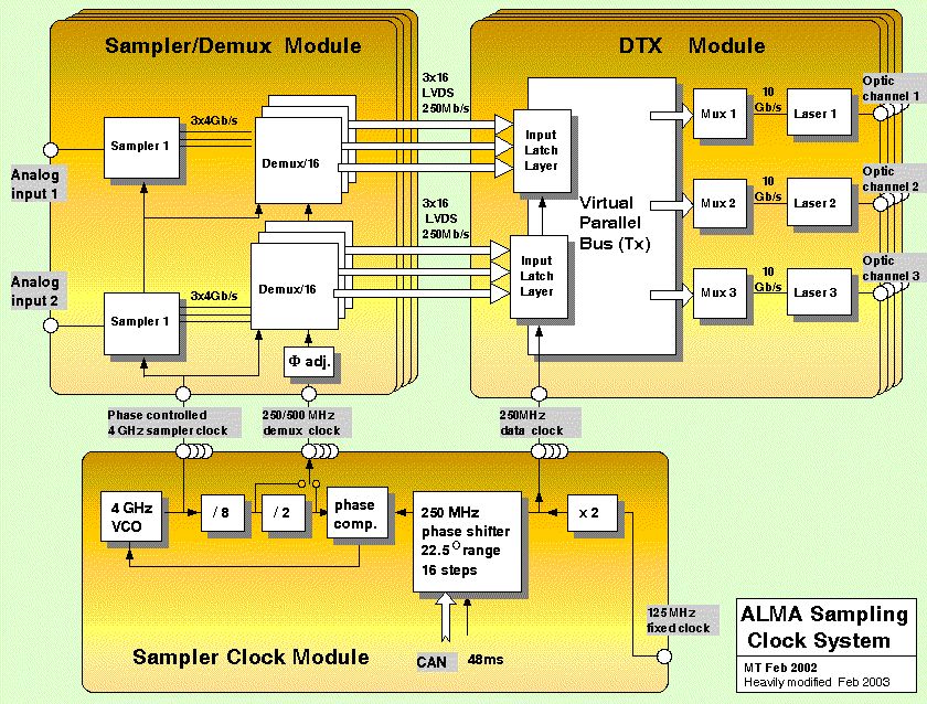
Fig.1 : Clock location in the sampler-related electronics
Although 8 steps are sufficient, the following designs will aim at
16
steps, because electronics that can offer the required accuracy for the
steps are de facto capable of providing more steps for
very
little additional cost.
So the engineering problem can be formulated as follows:
- Generate two 250 analog MHz signals, with relative phase
ranging
from 0 to 22.50 degrees, in 16 equally spaced steps, 1.40 +/- 0.15
degrees,
and then multiply the variable one by 16 so as to obtain a 16-PSK
constellation
at 4 GHz.
2. Analog solutions
There are several ways of implementing such a phase shift
at
250 MHz.
1. Varactor-tuned resonant circuit-loaded 3dB
hybrids.
This solution has been built in series (30 pcs) in an LO3 for the
previous
generation PdB correlator (1992). An E2PROM lookup table was
needed
to correct for their non linearity. A software using the correlator as
a phase meter was used to built and upload the lookup table. Although
the
requirement was quite modest (3 degrees @ 820MHz), they needed frequent
recalibration.
2. Digital timing ICs. Some all-digital chips
make
use of many individual gate propagation delays, together with
multiplexers,
to create substantial programmable delays. As many as 1024 gates can be
concatenated. This solution was tested in the lab many years ago but
was
never applied. The current candidate chip for this task is the Onsemi
EP195
. This solution probably does not offer sufficient quality for our
application.
3. I/Q modulators. These chips synthesize a vector of
any
phase by applying its Cartesian coordinates as voltages on their X and
Y inputs. They have the problems that generally affect analog devices,
which are drift and non-linearity. Several years ago, a student at IRAM
has worked out correction formulae taking into account a non-orthogonal
vector basis. This can remove the first-order distorsion quite well but
the instability is still present, especially at those 4 points of the
circle
where zero is applied on X or Y. This is due to the imperfect balance
of
the Gilbert cells inside the chips. However our application requires
that
we operate them in a small sector of the circle, and we can take
advantadge
of this by choosing an operating point where the slope of the actual
transfer
function is less sensitive to imperfections, e.g. at X=Y= 0.707.
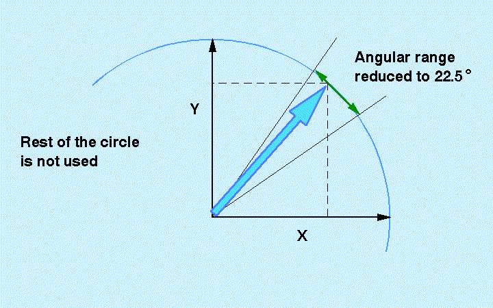
Fig.2: I/Q synthesis on a reduced phase range
If the Y (differential) connections are swapped and connected to
the
X ones, single-dimension operation can result on the tangential (green)
segment of Fig.2 . A good 12-bit D-to-A converter, followed by a lookup
correction table, can provide adequate resolution and accuracy.
Currently
available modulators are the Analog Devices AD8345 and Sirenza STQ1016.
Problems associated with this scheme come from the correction tables.
They need to be built up first, and this implies that a more
accurate
lab equipment setup is available. Tables will need to be personalized,
and this is a time-consuming process. It is likely that aging will
require
further recalibration. On a remote site this might not be practical.
3. Digital solution
Engineers use to experience a lot of
relief
when things can go digital. The DDS technique is extremely appropriate
for synthesising frequencies and phases. DDS has the inconvenience of
generating
a fairly high noise floor which in our case would be raised by the
multiply-up
factor, which is 24 dB. This noise floor is actually pseudo noise that
originates in the glitches of the D-to-A converter, which are
spread
across extremely long sequences. For some "happy frequencies" which are
submultiples of the clock frequency, the sequence repetition length is
exactly equal to one cycle of the generated sinewave, so the glitch
energy
gets tranformed into harmonics rather than pseudonoise.
A convenient frequency setup for generating the two sinewaves we
need
is Fclock=125 MHz, Fout=Fclock/16.
An analog filter is necessary to convert the staircase wave generated
by the D-to A into an unaliased sinewave. In our case it could be a
bandpass
filter, with a moderate penalty on the overall settling time.
The D-to-A's are clocked at 125 MHz, and receive their data from two
lookup tables, which are addressed by two 8-bit registers. Those two
registers
share the same 4 MSB's which come from a rolling accumulator, which
provides
the main frequency of 7.8125 MHz. The addition of LSB's to one of
the registers acts as a phase Vernier which has a resolution of 2pi/256
. Four bits give a total phase excursion of 2pi/16.
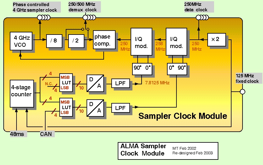
Fig.3 Functional block diagram of the clock module
The two sinewaves at 7.8125 MHz need to be translated to 250 MHz.
Two
I/Q modulators are used in an a "shift-up,shift-down" configuration.
The
AC-coupled use of those chips (opposed to DC-coupled, described above)
substantially reduces their two inconvenients:
Drift and aging still occur but the equal spacing of the phase steps
is preserved. The absolute value of the delay may vary slowly,
but
this will be taken out by calibration on sky sources (e.g. like antenna
deformations).
Non-linearity happens to be swept at the AC frequency so the small
deviations from the ideal,linear transfer function of the I/Q modulator
are exported to an harmonic of this frequency (see annex
1).
With the frequency values of Fig.3, lines can be expected at
258,266,274
MHz... and also 242,234... but they will be filtered by the x16
PLL
with a slope of 12 dB/octave. With 200kHz of loopBW, a delta of 7 MHz
is
rejected by 60dB. As long as the PLL is locked to the "nice
and clean" line, it will transfer its accurately synthesized phase
variations
to the 4 GHz VCO. For the lock-in to be safe, 20 dB spurious ratio is
sufficient.
This seems to be achievable and reproductible without excesssive
development.